 English
 Afrikaans
 العربية
 বাংলা
বাংলা bosanski jezik
 Български
 Català
 粤语
粤语 中文(简体)
 中文(漢字)
 Hrvatski
 Čeština
 Nederlands
 Eesti keel
 Suomi
Suomi Français
 Deutsch
 Ελληνικά
 हिन्दी; हिंदी
 Magyar
 Bahasa Indonesia
 Italiano
 日本語
日本語 한국어
한국어 Latviešu valoda
 Lietuvių kalba
 македонски јазик
 Bahasa Melayu
 Norsk
Norsk پارسی
پارسی Polski
 Português
 Română
 Русский
 Cрпски језик
 Slovenčina
 Slovenščina
 Español
 Svenska
 ภาษาไทย
 Türkçe
 Українська
 اردو
اردو Tiếng Việt
DS18B20 е цифров температурен сензор, който използва синхронизиране на една шина, за да комуникира с хоста. само 1 Необходим е проводник, за да завършите отчитането на температурните данни;
DS18B20 има вграден 64-битов сериен номер на продукта за лесна идентификация. Могат да бъдат свързани множество сензори DS18B20 1 Тел, и чрез 64-битово удостоверяване на самоличността, информацията за температурата, събрана от различни сензори, може да се чете отделно.
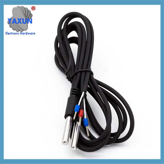 DS18B20 Комплект сонда от неръждаема стомана за измерване на температура |
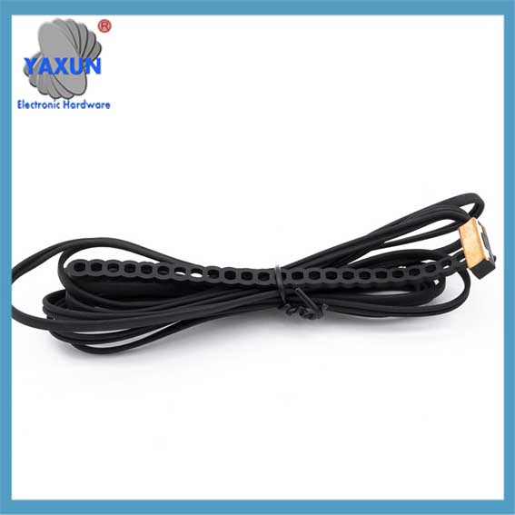 DS18B20 сонда за температурен сензор TPE Комплект за формоване |
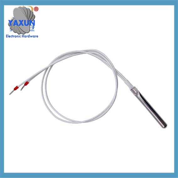 1 проводник DS18B20 температурен датчик |
Въведение в DS18B20
2.1 Основни характеристики на DS18B20
1. Напълно цифрово преобразуване и изход на температурата.
2. Усъвършенствана комуникация на данни с една шина.
3. До 12-битова резолюция, с точност до ±0,5 градуса по Целзий.
4. Максималният работен цикъл при 12-битова резолюция е 750 милисекунди.
5. Може да се избере паразитен режим на работа.
6. Температурният диапазон на откриване е –55°C ~+125°C (–67°F ~+257°F).
7. Вграден EEPROM, алармена функция за ограничаване на температурата.
8. 64-битова фотолитография ROM, вграден сериен номер на продукта, удобен за свързване на няколко машини.
9. Различни форми на опаковане, адаптиране към различни хардуерни системи.
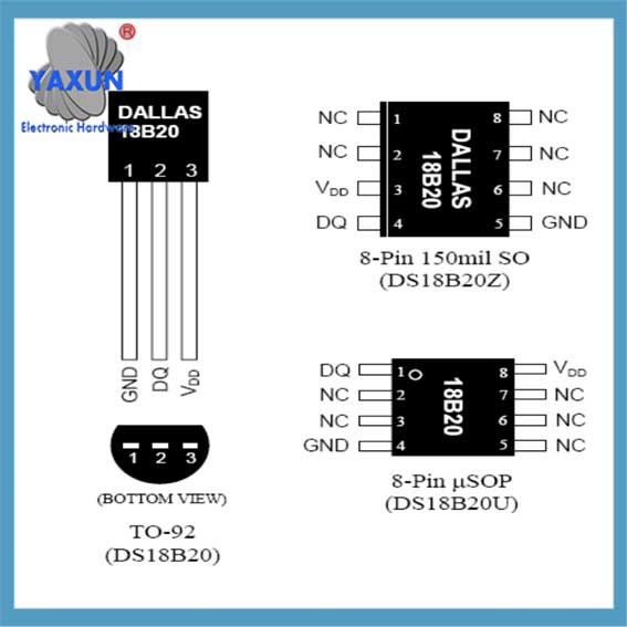
Структура на пакета на чип DS18B20
2.2 DS18B20 пин функция
GND напрежение земя;
DQ единична шина за данни;
VDD захранващо напрежение;
NC празен щифт;
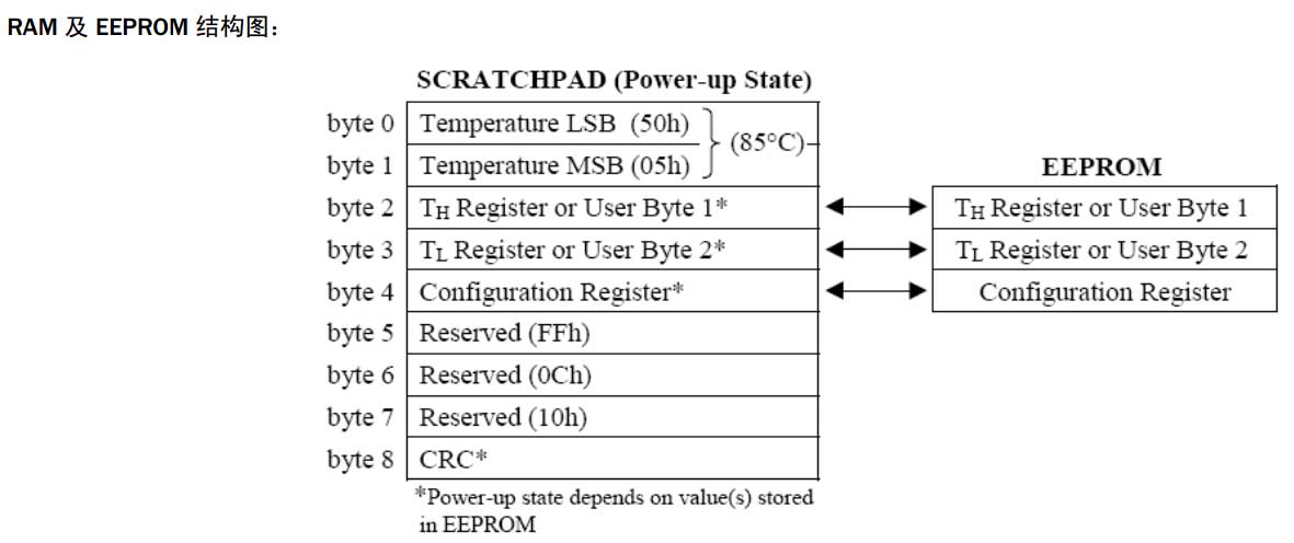
Структурна схема на RAM и EEPROM чип DS18B20
2.3 Принцип на работа и приложение на DS18B20
Откриването на температурата DS18B20 и цифровият изход на данни са напълно интегрирани в един чип, така че има по-силна способност против смущения. Неговият един работен цикъл може да бъде разделен на две части, а именно откриване на температура и обработка на данни.
18B20 има три форми на ресурси на паметта. Те са: ROM памет само за четене, използва се за съхраняване на DS18B20ID код; първият 8 битовете са едноредов сериен код (Кодът DS18B20 е 19H), следното 48 битовете са уникалният сериен номер на чипа; последният 8 битовете са CRC кодът (проверка за излишък) от горните 56 битове. Данните са зададени при производството и не могат да бъдат променяни от потребителя. DS18B20 има общо 64 битове ROM.
RAM регистър на данни, използвани за вътрешни изчисления и достъп до данни, данните се губят след спиране на захранването, DS18B20 има общо 9 байтове RAM, всеки байт е 8 битове. Първият и вторият байт са информацията за стойността на данните след преобразуване на температурата; третият и четвъртият байт са огледален образ на EEPROM на потребителя (обикновено се използва за съхранение на стойност на алармата за температура). Стойността му ще се обнови при нулиране на захранването. Петият байт е огледален образ на третата EEPROM на потребителя. 6-тото, 7th, и 8-ми байтове са регистри за броене, които са предназначени да позволят на потребителите да получат по-висока температурна разделителна способност. Те също така са единици за временно съхранение за вътрешно преобразуване и изчисляване на температурата. 9-ият байт е CRC кодът на първия 8 байтове. EEPROM е енергонезависима памет, използвана за съхраняване на данни, които трябва да бъдат запазени за дълго време, алармени стойности за горна и долна температура, и данни за проверка. DS18B20 има общо 3 битове от EEPROM, и има огледални изображения в RAM за улесняване на работата на потребителя.
DS18B20 работи в режим на 12-битова резолюция по подразбиране. 12-битовите данни, получени след преобразуването, се съхраняват в две 8-битови RAM на DS18B20 (първите два байта). Първият 5 битовете в двоичната система са знакови битове. Ако измерената температура е по-висока от 0, тези 5 бита са 0. Просто умножете измерената стойност по 0.0625 за да получите действителната температура. Ако температурата е по-ниска от 0, тези 5 бита са 1. Измерената стойност трябва да се обърне, добавен от 1, и след това умножено по 0.0625 за да получите действителната температура. Или използвайте битова операция за извличане на температура: десетичните знаци заемат долната 4 битове, а горните битове са цели числа (отрицателните числа не се вземат предвид).
2.4 Таблица с инструкции за ROM чип DS18B20
1. Прочетете ROM [33З] (шестнадесетичната командна дума е в квадратни скоби).
Тази команда позволява на контролера на шината да чете 64-битовия ROM на DS18B20. Тази инструкция може да се използва само когато има само един DS18B20 в шината. Ако са свързани повече от един, ще възникнат конфликти на данни по време на комуникация.
2. atch ROM [55З]
Тази инструкция е последвана от 64-битов сериен номер, издаден от контролера. Когато има няколко DS18B20 в шината, може да отговори само чипът със същия сериен номер като този, издаден от контролера, и другите чипове ще изчакат следващото нулиране. Тази инструкция е подходяща за свързване с един чип и много чипове.
3. Пропуснете ROM [CCH]
Тази инструкция кара чипа да не реагира на ROM кода. В случай на един автобус, тази инструкция може да се използва за спестяване на време. Ако тази инструкция се използва, когато са свързани множество чипове, ще възникнат конфликти на данни, което води до грешки.
4. Търсене в ROM [F0H]
След инициализиране на чипа, инструкцията за търсене позволява 64-битовата ROM на всички устройства да бъде идентифицирана чрез елиминиране, когато множество чипове са свързани към шината.
5. Търсене на аларма [ВСЯКА]
В случай на множество чипове, инструкцията за търсене на алармен чип отговаря само на чипове, които отговарят на аларменото условие за температура, по-висока от TH или по-ниска от TL. Докато чипът не е изключен, аларменото състояние ще се поддържа, докато температурата не бъде измерена отново и аларменото състояние не бъде достигнато.
6. Напишете Scratchpad [4ЕХ]
Това е инструкцията за запис на данни в RAM. Двата байта данни, записани впоследствие, ще бъдат съхранени на адрес 2 (TH на алармата RAM) и адрес 3 (TL на алармата RAM). Процесът на запис може да бъде прекратен чрез сигнал за нулиране.
7. Прочетете Scratchpad (чете данни от RAM) [БЕХ]
Тази инструкция ще чете данни от RAM, започвайки от адрес 0 и до адрес 9, завършване на четенето на всички RAM данни. Чипът позволява на сигнала за нулиране да прекрати процеса на четене, това е, следващите ненужни байтове могат да бъдат игнорирани, за да се намали времето за четене.
8. Копиране на Scratchpad (копирайте RAM данни в EEPROM) [48З]
Тази инструкция съхранява данните в RAM в EEPROM, така че данните да не бъдат загубени при изключване на захранването. Тъй като чипът е зает с обработка на съхранение на EEPROM, когато контролерът изпрати времеви интервал за четене, изходите на шината “0”, и когато работата по съхранението приключи, шината ще изведе “1”.
В паразитен режим на работа, трябва да се използва силно издърпване веднага след издаването на тази инструкция и да се поддържа поне 10MS, за да се поддържа работата на чипа.
9. Преобразувайте Т (преобразуване на температурата) [44З]
След получаване на тази инструкция, чипът ще извърши преобразуване на температурата и ще съхрани преобразуваната стойност на температурата в 1-ви и 2-ри адрес на RAM. Тъй като чипът е зает с обработка на преобразуване на температурата, когато контролерът изпрати времеви интервал за четене, изходите на шината “0”, и когато работата по съхранението приключи, шината ще изведе “1”. В паразитен режим на работа, трябва да се използва силно издърпване веднага след издаването на тази инструкция и да се поддържа поне 500MS, за да се поддържа работата на чипа.
10. Извикайте EEPROM (Копирайте стойността на алармата в EEPROM в RAM) [B8H]
Тази инструкция копира стойността на алармата в EEPROM в 3-тия и 4-тия байт в RAM. Тъй като чипът е зает с обработка на копиране, когато контролерът изпрати времеви интервал за четене, изходите на шината “0”, и когато работата по съхранението приключи, изходите на шината “1”. Освен това, тази инструкция ще се изпълни автоматично, когато чипът се включи и нулира. По този начин, двата алармени бита в RAM винаги ще бъдат огледален образ на данните в EEPROM.
11. Прочетете захранването (Превключвател за режим на работа) [B4H]
След издаване на тази инструкция, издава се интервал от време за четене, и чипът ще върне своята дума за статус на захранване. “0” е паразитното състояние на властта и “1” е състоянието на външна мощност.
2.5 DS18B20 Времева диаграма
2.5.1 DS18B20 Диаграма на връзката за нулиране и реакция
Преди всяка комуникация трябва да се извърши нулиране. Времето за нулиране, време на изчакване, и времето за реакция трябва да бъде стриктно програмирано според времето.
Разлика във времето за четене и запис на DS18B20: Четенето и записването на данни DS18B20 се потвърждава от бита за обработка на интервала във времето и командната дума за обмен на информация.

Диаграма на връзката между нулиране и реакция на DS18B20
2.5.2 Запишете данни 0 и данни 1 към DS18B20
В първите 15uS от интервала от време за запис на данни, шината трябва да бъде изтеглена ниско от контролера, и тогава ще бъде времето за вземане на проби от чипа за данните от шината. Времето за вземане на проби е 15~60uS. Ако контролерът издърпа шината високо по време на времето за вземане на проби, това означава писане “1”, и ако контролерът дръпне шината ниско, това означава писане “0”.
Всеки бит на предаване трябва да има начален бит на ниско ниво от поне 15uS, и последващите данни “0” или “1” трябва да бъде завършен в рамките на 45uS.
Времето за предаване на целия бит трябва да се поддържа на 60~120uS, в противен случай нормалната комуникация не може да бъде гарантирана.
Забележка: DS18B20 чете и записва данни от ниския бит.
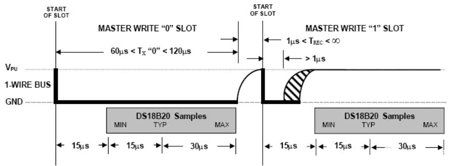
Запишете данни 0 и данни 1 към DS18B20
2.5.3 Четене на данни 0 и данни 1 от DS18B20
Времето за вземане на проби от контролата по време на празнината във времето за четене трябва да бъде по-точно. По време на празнината във времето за четене, хостът трябва също така да генерира ниско ниво от поне 1uS, за да покаже началото на времето за четене. Тогава, в 15uS след освобождаването на автобуса, DS18B20 ще изпрати вътрешния бит за данни. По това време, ако контролът установи, че шината е висока, това означава четене “1”, и ако автобусът е нисък, това означава четене на данни “0”. Преди да прочетете всеки бит, контролерът добавя стартов сигнал.
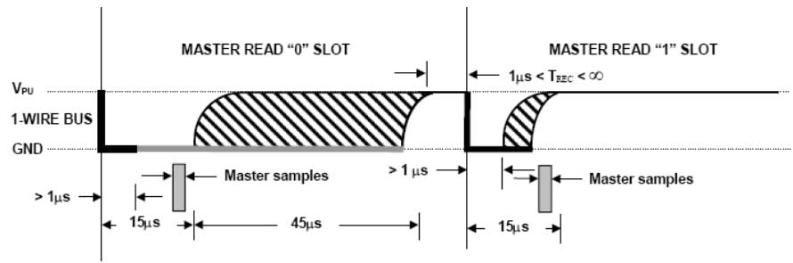
Прочетете данни 0 и данни 1 от DS18B20
Забележка: Битът за данни трябва да бъде прочетен в рамките на 15uS от началото на интервала за четене, за да се осигури правилна комуникация.
По време на комуникация, 8 парченца от “0” или “1” се използват като байт, и четенето или записването на байта започва от ниския бит.
2.5.4 Ред на еднократно отчитане на температурата (само един DS18B20 в автобуса)
1. Изпратете сигнал за нулиране
2. Откриване на сигнал за отговор
3. Изпратете 0xCC
4. Изпратете 0x44
5. Изпратете сигнал за нулиране
6. Откриване на сигнал за отговор
7. Напишете 0xcc
8. Напишете 0xbe
9. Цикъл 8 пъти, за да прочетете ниския байт на температурата
10. Цикъл 8 пъти, за да прочетете високия байт на температурата
11. Синтезирайте 16-битови температурни данни и обработете
3. Код на водача
3.1 DS18B20.c
#включват “ds18b20.h”
/*
функция: Инициализация на DS18B20
Хардуерна връзка: PB15
*/
void DS18B20_Инициал(невалиден)
{
RCC->APB2ENR|=1<<3; //PB
GPIOB->CRH&=0x0FFFFFFF;
GPIOB->CRH|=0x30000000;
GPIOB->ODR|=1<<15; //Набиране
}
/*
функция: Проверете дали устройството DS18B20 съществува
Върната стойност: 1 означава, че устройството не съществува 0 означава, че устройството е нормално
*/
u8 DS18B20_CheckDevice(невалиден) //Съдържа импулс за нулиране, импулс за откриване
{
DS18B20_РЕЖИМ НА ИЗХОД();//Инициализиране в изходен режим
DS18B20_OUT=0; //Генериране на импулс за нулиране
DelayUs(750); //Генерирайте 750us ниско ниво
DS18B20_OUT=1; //Освободете автобуса
DelayUs(15); //Изчакайте отговора на DS18B20
ако(DS18B20_CleckAck())//Откриване на импулс на съществуване
{
връщане 1;
}
връщане 0;
}
/*
функция: Откриване на импулс за съществуване на устройство DS18B20
Върната стойност: 1 показва грешка 0 показва нормално
*/
u8 DS18B20_CleckAck(невалиден)
{
u8 cnt=0;
DS18B20_INPUT_MODE();//Инициализиране към режим на въвеждане
докато(DS18B20_IN&&cnt<200) //Изчакайте импулс за съществуване на отговор на DS18B20
{
DelayUs(1);
cnt++;
}
ако(cnt>=200)връщане 1; //грешка
cnt=0;
докато((!DS18B20_IN)&&cnt<240) //изчакайте DS18B20 да освободи шината
{
DelayUs(1);
cnt++;
}
ако(cnt>=240)връщане 1; //грешка
връщане 0;
}
/*
функция: Напишете байт
Първо се научи да пишеш малко.
*/
void DS18B20_WriteByte(u8 cmd)
{
u8 i;
DS18B20_РЕЖИМ НА ИЗХОД(); //Инициализиране в изходен режим
за(i=0;аз<8;i++)
{
DS18B20_OUT=0; //Генериране на празнина във времето за запис (пишете начало)
DelayUs(2);
DS18B20_OUT=cmd&0x01; //Изпращане на действителни данни
DelayUs(60); //Изчакайте завършването на записа
DS18B20_OUT=1; //Освободете автобуса и се подгответе за следващото предаване
cmd>>=1; //Продължете да изпращате следващия бит данни
}
}
/*
функция: Прочетете байт
Първо се научи да четеш малко.
*/
u8 DS18B20_ReadByte(невалиден)
{
u8 i,данни=0;
за(i=0;аз<8;i++)
{
DS18B20_РЕЖИМ НА ИЗХОД(); //Инициализиране в изходен режим
DS18B20_OUT=0; //Генерирайте празнина във времето за четене (начало на четене)
DelayUs(2);
DS18B20_OUT=1; //Освободете автобуса
DS18B20_INPUT_MODE(); //Инициализиране към режим на въвеждане
DelayUs(8); //Изчакайте извеждането на данни от DS18B20
данни>>=1; //Напълнете високия бит с 0, по подразбиране е 0
ако(DS18B20_IN) данни|=0x80;
DelayUs(60);
DS18B20_OUT=1; //Освободете автобуса, изчакайте за четене на следващия бит от данни
}
върнати данни;
}
/*
функция: Прочетете температурните данни на DS18B20 веднъж
Върната стойност: данните за температурата се четат
Обмислена ситуация: Има само един DS18B20, свързан към шината
*/
u16 DS18B20_ReadTemp(невалиден)
{
u16 температура = 0;
u8 temp_H,temp_L;
DS18B20_CheckDevice(); //Изпратете импулс за нулиране, откриване на пулса
DS18B20_WriteByte(0xCC); //Пропуснете откриването на ROM последователност
DS18B20_WriteByte(0x44); //Започнете преобразуване на температурата
//Изчакайте преобразуването на температурата да завърши
докато(DS18B20_ReadByte()!=0xFF){}
DS18B20_CheckDevice(); //Изпратете импулс за нулиране, откриване на пулса
DS18B20_WriteByte(0xCC); //Пропуснете откриването на ROM последователност
DS18B20_WriteByte(0xBE); //Прочетете температурата
temp_L=DS18B20_ReadByte(); //Прочетете данни за ниска температура
temp_H=DS18B20_ReadByte(); //Прочетете данни за висока температура
температура=temp_L|(temp_H<<8); //Синтезирана температура
връщане темп;
}
3.2 DS18B20.h
#ifndef DS18B20_H
#дефинирайте DS18B20_H
#включват “stm32f10x.h”
#включват “sys.h”
#включват “забавяне.ч”
#включват “ds18b20.h”
#включват “usart.h”
/*Интерфейс на пакета*/
//Инициализирайте DS18B20 в режим на въвеждане
#дефинирайте DS18B20_INPUT_MODE() {GPIOB->CRH&=0x0FFFFFFF;GPIOB->CRH|=0x80000000;}
//Инициализирайте DS18B20 в изходен режим
#дефинирайте DS18B20_OUTPUT_MODE(){GPIOB->CRH&=0x0FFFFFFF;GPIOB->CRH|=0x30000000;}
//DS18B20 IO порт изход
#дефинирайте DS18B20_OUT PBout(15)
//DS18B20 IO порт вход
#дефинирайте DS18B20_IN PBin(15)
//Декларация на функция
u8 DS18B20_CleckAck(невалиден);
u8 DS18B20_CheckDevice(невалиден);
void DS18B20_Инициал(невалиден);
u16 DS18B20_ReadTemp(невалиден);
u8 DS18B20_ReadByte(невалиден);
void DS18B20_WriteByte(u8 cmd);
#endif
poYBAGDYdXCAWkKMAAAAK8RNs4s030.png
3.3 Функция забавяне
/*
функция: Закъснение в нас
*/
невалидни DelayUs(int us)
{
#ifdef _SYSTICK_IRQ_
int i,й;
за(i=0;iVAL=0; //CNT стойност на брояча
SysTick->ЗАРЕЖДАНЕ=9*нас; //9 означава 1us
SysTick->CTRL|=1<<0; //Стартирайте таймера
направете
{
tmp=SysTick->CTRL; //Прочетете състоянието
}докато((!(tmp&1<<16))&&(tmp&1<<0));
SysTick->VAL=0; //CNT стойност на брояча
SysTick->CTRL&=~(1<<0); //Изключете таймера
#endif
};i++)>
3.4 main.c Обадете се на DS18B20, за да прочетете температурата и да я отпечатате на серийния порт
#включват “stm32f10x.h”
#включват “ds18b20.h”
u8 DS18B20_ROM[8]; //Съхранявайте 64-битовия ROM код на DS18B20
int main(невалиден)
{
u16 темп;
USARTx_Heat(USART1,72,115200);//Инициализация на сериен порт 1
DS18B20_Топлина(); //Инициализация на DS18B20
/*1. Прочетете 64-битовия ROM код на DS18B20*/
//Изпратете импулс за нулиране, откриване на пулса на съществуване
докато(DS18B20_CheckDevice())
{
printf(“Устройство DS18B20 не съществува!\п”);
DelayMs(500);
}
//Изпратете командата за четене на 64-битовия ROM код
DS18B20_WriteByte(0x33);
//Цикъл за четене на 64-битов ROM код
за(i=0;аз<8;i++)
{
DS18B20_ROM[аз]= DS18B20_ReadByte();
printf(“DS18B20_ROM[%d]=0x%Xn”,аз,DS18B20_ROM[аз]);
}
докато(1)
{
/*2. Едновременно работете с всички DS18B20 в шината, за да започнете преобразуване на температурата*/
DS18B20_CheckDevice(); //Изпратете импулс за нулиране, откриване на пулса
DS18B20_WriteByte(0xCC); //Пропуснете откриването на ROM последователност
DS18B20_WriteByte(0x44); //Започнете преобразуване на температурата (нека всички DS18B20 в шината преобразуват температурата)
DelayMs(500); //Изчакайте всички температурни преобразувания на DS18B20 по линията да завършат
/*3. Единично целево отчитане на температурата на всеки DS18B20*/
DS18B20_CheckDevice(); //Изпратете импулс за нулиране, откриване на пулса
DS18B20_WriteByte(0x55); //Изпратете команда за съответствие с ROM
за(i=0;аз<8;i++) //Изпратете 64-битов код
{
DS18B20_WriteByte(DS18B20_ROM[аз]);
}
DS18B20_WriteByte(0xBE); //Прочетете температурата
temp=DS18B20_ReadByte(); //Прочетете температурни данни от нисък порядък
Темп|=DS18B20_ReadByte()<<8; //Прочетете температурни данни от висок порядък
printf(“temp1=%d.%dn”,Темп>>4,Темп&0xF);
printf(“temp2=%fn”,температура*0,0625);
DelayMs(500);
}
}