 English
 Afrikaans
 العربية
 বাংলা
বাংলা bosanski jezik
 Български
 Català
 粤语
粤语 中文(简体)
 中文(漢字)
 Hrvatski
 Čeština
 Nederlands
 Eesti keel
 Suomi
Suomi Français
 Deutsch
 Ελληνικά
 हिन्दी; हिंदी
 Magyar
 Bahasa Indonesia
 Italiano
 日本語
日本語 한국어
한국어 Latviešu valoda
 Lietuvių kalba
 македонски јазик
 Bahasa Melayu
 Norsk
Norsk پارسی
پارسی Polski
 Português
 Română
 Русский
 Cрпски језик
 Slovenčina
 Slovenščina
 Español
 Svenska
 ภาษาไทย
 Türkçe
 Українська
 اردو
اردو Tiếng Việt
DS18B20 är en digital temperatursensor som använder en enda busstiming för att kommunicera med värden. Endast 1 Kabel behövs för att slutföra temperaturdataavläsningen;
DS18B20 har ett inbyggt 64-bitars produktserienummer för enkel identifiering. Flera DS18B20-sensorer kan anslutas till 1 Tråd, och genom 64-bitars identitetsautentisering, temperaturinformationen som samlas in från olika sensorer kan läsas separat.
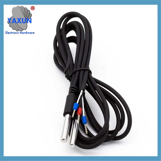 DS18B20 temperaturavkännande tråd i rostfritt stål |
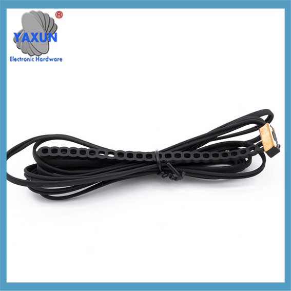 DS18B20 temperaturgivare sond TPE övergjutningssats |
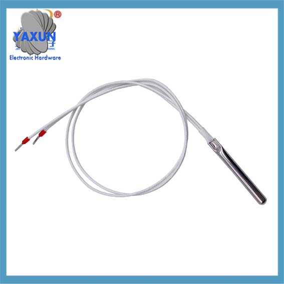 1 tråd DS18B20 temperaturgivare |
Introduktion till DS18B20
2.1 Huvudfunktioner hos DS18B20
1. Helt digital temperaturomvandling och utgång.
2. Avancerad enkelbuss datakommunikation.
3. Upp till 12-bitars upplösning, med en noggrannhet på upp till ±0,5 grader Celsius.
4. Den maximala arbetscykeln vid 12-bitars upplösning är 750 millisekunder.
5. Parasitiskt arbetsläge kan väljas.
6. Detekteringstemperaturområdet är –55°C ~+125°C (–67° F ~+257° F).
7. Inbyggt EEPROM, temperaturgräns larmfunktion.
8. 64-bit fotolitografi ROM, inbyggt produktserienummer, bekvämt för multimaskinanslutning.
9. Olika förpackningsformer, anpassa sig till olika hårdvarusystem.
DS18B20-chippaketstruktur
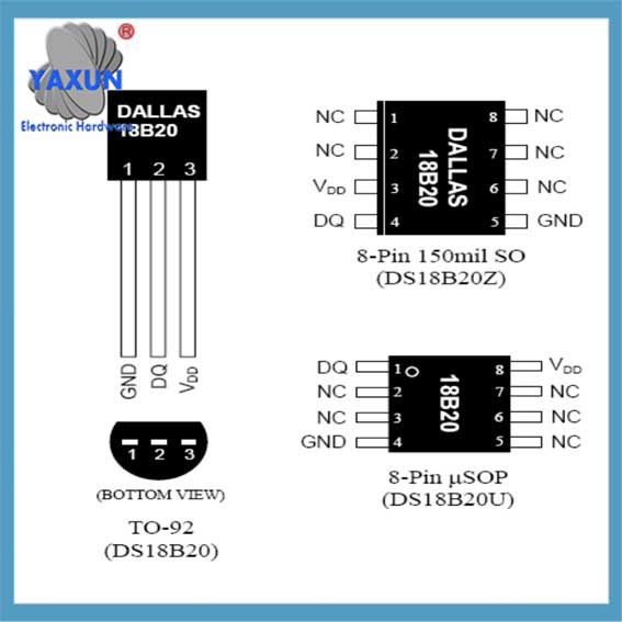
2.2 DS18B20 stiftfunktion
GND spänning jord;
DQ enkel databuss;
VDD strömförsörjningsspänning;
NC tom stift;
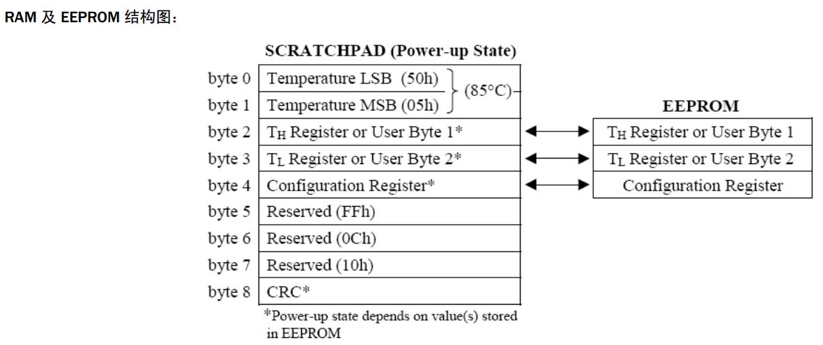
DS18B20 chip RAM och EEPROM strukturdiagram
2.3 DS18B20 arbetsprincip och tillämpning
DS18B20 temperaturdetektering och digital datautgång är helt integrerade på ett chip, så den har starkare anti-interferensförmåga. Dess ena arbetscykel kan delas upp i två delar, nämligen temperaturdetektering och databehandling.
18B20 har tre former av minnesresurser. Det är de: ROM skrivskyddat minne, används för att lagra DS18B20ID-kod; den första 8 bitar är en rads seriekod (DS18B20-koden är 19H), följande 48 bitar är chipets unika serienummer; den sista 8 bitar är CRC-koden (redundanskontroll) av ovanstående 56 bitar. Data ställs in vid produktion och kan inte ändras av användaren. DS18B20 har totalt 64 bitar av ROM.
RAM-dataregister, används för intern beräkning och dataåtkomst, data går förlorade efter strömavbrott, DS18B20 har totalt 9 byte RAM, varje byte är 8 bitar. Den första och andra byten är datavärdesinformationen efter temperaturomvandling; den tredje och fjärde byten är spegelbilden av användarens EEPROM (används vanligtvis för lagring av temperaturlarmvärden). Dess värde kommer att uppdateras när strömmen återställs. Den femte byten är spegelbilden av användarens tredje EEPROM. Den 6:e, 7th, och 8:e byte är räkningsregister, som är designade för att tillåta användare att få högre temperaturupplösning. De är också tillfälliga lagringsenheter för intern temperaturomvandling och beräkning. Den 9:e byten är CRC-koden för den första 8 bytes. EEPROM är ett icke-flyktigt minne som används för att lagra data som behöver sparas under lång tid, övre och nedre temperaturlarmvärden, och verifieringsdata. DS18B20 har totalt 3 bitar av EEPROM, och det finns spegelbilder i RAM-minnet för att underlätta användarens användning.
DS18B20 fungerar som standard i 12-bitars upplösningsläge. 12-bitars data som erhålls efter konvertering lagras i två 8-bitars RAM-minnen på DS18B20 (de två första byten). Den första 5 bitar i binär är teckenbitar. Om den uppmätta temperaturen är högre än 0, dessa 5 bitar är 0. Multiplicera bara det uppmätta värdet med 0.0625 för att få den faktiska temperaturen. Om temperaturen är lägre än 0, dessa 5 bitar är 1. Det uppmätta värdet måste inverteras, tillagd av 1, och sedan multipliceras med 0.0625 för att få den faktiska temperaturen. Eller använd bitdrift för att extrahera temperatur: decimalerna upptar den lägre 4 bitar, och de övre bitarna är heltalsbitar (negativa tal beaktas inte).
2.4 DS18B20 chip ROM instruktionstabell
1. Läs rom [33H] (det hexadecimala kommandoordet står inom hakparenteser).
Detta kommando gör att bussstyrenheten kan läsa 64-bitars ROM i DS18B20. Denna instruktion kan endast användas när det bara finns en DS18B20 på bussen. Om mer än en är ansluten, datakonflikter kommer att uppstå under kommunikation.
2. atch ROM [55H]
Denna instruktion följs av ett 64-bitars serienummer utfärdat av styrenheten. När det finns flera DS18B20 på bussen, endast chippet med samma serienummer som det som utfärdats av styrenheten kan svara, och de andra markerna väntar på nästa återställning. Denna instruktion är lämplig för enkelchips- och multi-chipanslutning.
3. Skeppsrum [CCH]
Denna instruktion gör att chipet inte svarar på ROM-koden. När det gäller en enda buss, denna instruktion kan användas för att spara tid. Om denna instruktion används när flera chips är anslutna, datakonflikter kommer att uppstå, resulterar i fel.
4. Sök ROM [F0H]
Efter att chippet har initierats, sökinstruktionen gör att 64-bitars ROM för alla enheter kan identifieras genom eliminering när flera chips är anslutna till bussen.
5. Larmsökning [VARJE]
I fallet med flera marker, larmchipssökningsinstruktionen svarar endast på chips som uppfyller larmvillkoret för temperatur högre än TH eller lägre än TL. Så länge chippet inte är avstängt, larmtillståndet kommer att bibehållas tills temperaturen mäts igen och larmtillståndet inte uppnås.
6. Skriv skrapplatta [4VA]
Detta är instruktionen för att skriva data till RAM. De två bytes med data som skrivs efteråt kommer att lagras på adressen 2 (TH av larm-RAM) och adress 3 (TL för larm-RAM). Skrivprocessen kan avslutas med en återställningssignal.
7. Läs Scratch Pad (läsa data från RAM) [BEH]
Denna instruktion kommer att läsa data från RAM, med början från adress 0 och upp till adress 9, slutföra läsningen av hela RAM-data. Chipet tillåter återställningssignalen att avsluta läsningsprocessen, som är, de efterföljande onödiga byten kan ignoreras för att minska lästiden.
8. Kopiera skrapplatta (kopiera RAM-data till EEPROM) [48H]
Denna instruktion lagrar data i RAM i EEPROM så att data inte kommer att gå förlorade när strömmen stängs av. Eftersom chippet är upptaget med EEPROM-lagringsbehandling, när styrenheten skickar en lästidlucka, bussutgångarna “0”, och när lagringsarbetet är klart, bussen kommer ut “1”.
I parasitiskt arbetsläge, en stark pull-up måste användas omedelbart efter att denna instruktion har utfärdats och underhållas i minst 10MS för att bibehålla chipdrift.
9. Konvertera T (temperaturomvandling) [44H]
Efter att ha fått denna instruktion, chippet kommer att utföra en temperaturomvandling och lagra det konverterade temperaturvärdet i den 1:a och 2:a adressen i RAM. Eftersom chipet är upptaget med temperaturomvandlingsbearbetning, när styrenheten skickar en lästidlucka, bussutgångarna “0”, och när lagringsarbetet är klart, bussen kommer ut “1”. I parasitiskt arbetsläge, en stark pull-up måste användas omedelbart efter att denna instruktion har utfärdats och underhålls i minst 500MS för att bibehålla chipdrift.
10. Återkalla EEPROM (Kopiera larmvärdet i EEPROM till RAM) [B8H]
Denna instruktion kopierar larmvärdet i EEPROM till 3:e och 4:e byten i RAM. Eftersom chippet är upptaget med kopieringsbearbetning, när styrenheten skickar en lästidlucka, bussutgångarna “0”, och när lagringsarbetet är klart, bussutgångarna “1”. Dessutom, denna instruktion kommer att köras automatiskt när chippet slås på och återställs. På det här sättet, de två larmbytebitarna i RAM kommer alltid att vara spegelbilden av data i EEPROM.
11. Läs Strömförsörjning (Omkopplare för arbetsläge) [B4H]
Efter denna instruktion utfärdas, ett lästidsgap utfärdas, och chippet kommer att returnera sitt effektstatusord. “0” är det parasitiska makttillståndet och “1” är det externa strömtillståndet.
2.5 DS18B20 Tidsdiagram
2.5.1 DS18B20 Återställnings- och svarsrelationsdiagram
En återställning måste utföras före varje kommunikation. Återställningstiden, väntetid, och svarstiden bör strikt programmeras enligt tidpunkten.
DS18B20 läs- och skrivtidsgap: DS18B20-dataläsning och -skrivning bekräftas av tidsgapbearbetningsbiten och kommandoordet för att utbyta information.

DS18B20 återställnings- och svarsförhållandediagram
2.5.2 Skriv data 0 och data 1 till DS18B20
Under de första 15uS av skrivdatatidgapet, bussen måste dras lågt av styrenheten, och då blir det chipsamplingstiden för bussdata. Provtagningstiden är 15~60uS. Om styrenheten drar bussen högt under samplingstiden, det betyder att skriva “1”, och om styrenheten drar bussen lågt, det betyder att skriva “0”.
Varje överföringsbit bör ha en startbit på låg nivå på minst 15uS, och efterföljande data “0” eller “1” bör slutföras inom 45uS.
Överföringstiden för hela biten bör hållas vid 60~120uS, annars kan den normala kommunikationen inte garanteras.
Notera: DS18B20 läser och skriver data från den låga biten.
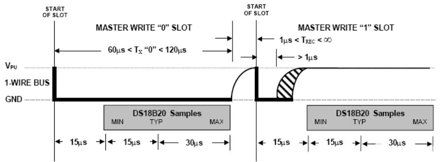
Skriv data 0 och data 1 till DS18B20
2.5.3 Läser data 0 och data 1 från DS18B20
Samplingstiden för kontrollen under avläsningstidsgapet bör vara mer exakt. Under lästidsgapet, värden måste också generera en låg nivå på minst 1uS för att indikera starten på lästiden. Sedan, om 15uS efter att bussen släppts, DS18B20 skickar den interna databiten. Just nu, om kontrollen upptäcker att bussen är hög, det betyder att läsa “1”, och om bussen är låg, det betyder att läsa data “0”. Innan du läser varje bit, regulatorn lägger till en startsignal.
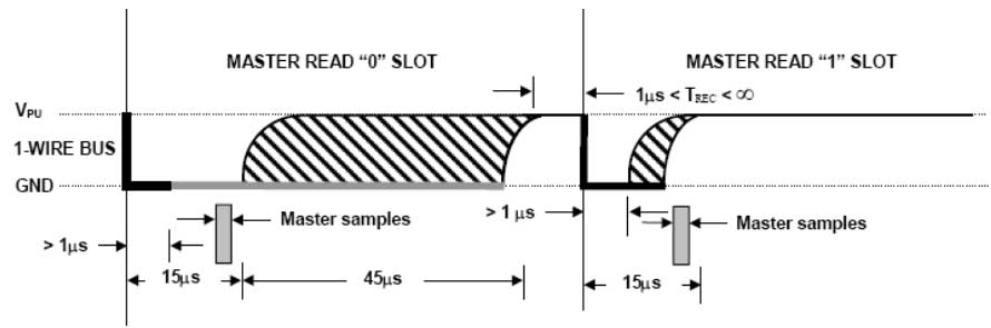
Läs data 0 och data 1 från DS18B20
Notera: Databiten måste läsas inom 15uS från början av läsgapet för att säkerställa korrekt kommunikation.
Under kommunikation, 8 bitar av “0” eller “1” används som en byte, och läsningen eller skrivningen av byten börjar från den låga biten.
2.5.4 Ordning för avläsning av temperatur en gång (bara en enda DS18B20 på bussen)
1. Skicka återställningssignal
2. Upptäck svarssignal
3. Skicka 0xCC
4. Skicka 0x44
5. Skicka återställningssignal
6. Upptäck svarssignal
7. Skriv 0xcc
8. Skriv 0xbe
9. Slinga 8 gånger för att läsa av temperaturens låga byte
10. Slinga 8 gånger för att läsa den höga byten av temperatur
11. Syntetisera 16-bitars temperaturdata och process
3. Förarens kod
3.1 DS18B20.c
#omfatta “ds18b20.h”
/*
Fungera: DS18B20 initiering
Hårdvaruanslutning: PB15
*/
ogiltig DS18B20_Init(ogiltig)
{
RCC->APB2ENR|=1<<3; //PB
GPIOB->CRH&=0x0FFFFFFF;
GPIOB->CRH|=0x30000000;
GPIOB->ODR|=1<<15; //Uppdrag
}
/*
Fungera: Kontrollera om DS18B20-enheten finns
Returvärde: 1 betyder att enheten inte finns 0 betyder att enheten är normal
*/
u8 DS18B20_CheckDevice(ogiltig) //Innehåller återställningspuls, detekteringspuls
{
DS18B20_OUTPUT_MODE();//Initiera till utgångsläge
DS18B20_OUT=0; //Generera återställningspuls
DelayUs(750); //Generera 750us låg nivå
DS18B20_OUT=1; //Släpp bussen
DelayUs(15); //Vänta på DS18B20-svar
om(DS18B20_CleckAck())//Upptäck existenspuls
{
återvända 1;
}
återvända 0;
}
/*
Fungera: Upptäck existenspuls för DS18B20-enhet
Returvärde: 1 indikerar fel 0 indikerar normalt
*/
u8 DS18B20_CleckAck(ogiltig)
{
u8 cnt=0;
DS18B20_INPUT_MODE();//Initiera till inmatningsläge
medan(DS18B20_IN&&cnt<200) //Vänta på DS18B20-svarsexistenspuls
{
DelayUs(1);
cnt++;
}
om(cnt>=200)återvända 1; //fel
cnt=0;
medan((!DS18B20_IN)&&cnt<240) //vänta på att DS18B20 ska släppa bussen
{
DelayUs(1);
cnt++;
}
om(cnt>=240)återvända 1; //fel
återvända 0;
}
/*
Fungera: Skriv en byte
Lär dig först hur man skriver lite.
*/
ogiltig DS18B20_WriteByte(u8 cmd)
{
u8 i;
DS18B20_OUTPUT_MODE(); //Initiera till utgångsläge
för(i=0;i<8;i++)
{
DS18B20_OUT=0; //Generera skrivtidsgap (skriva start)
DelayUs(2);
DS18B20_OUT=cmd&0x01; //Skicka faktisk databit
DelayUs(60); //Vänta tills skrivningen är klar
DS18B20_OUT=1; //Släpp bussen och förbered för nästa sändning
cmd>>=1; //Fortsätt att skicka nästa databit
}
}
/*
Fungera: Läs en byte
Lär dig först att läsa lite.
*/
u8 DS18B20_ReadByte(ogiltig)
{
u8 i,data=0;
för(i=0;i<8;i++)
{
DS18B20_OUTPUT_MODE(); //Initiera till utgångsläge
DS18B20_OUT=0; //Generera lästidsgap (lässtart)
DelayUs(2);
DS18B20_OUT=1; //Släpp bussen
DS18B20_INPUT_MODE(); //Initiera till inmatningsläge
DelayUs(8); //Vänta på DS18B20-datautmatning
data>>=1; //Fyll hög bit med 0, standard är 0
om(DS18B20_IN) data|=0x80;
DelayUs(60);
DS18B20_OUT=1; //Släpp bussen, vänta på att läsa nästa bit data
}
returnera data;
}
/*
Fungera: Läs temperaturdata för DS18B20 en gång
Returvärde: avlästa temperaturdata
Övervägd situation: Det finns bara en DS18B20 ansluten till bussen
*/
u16 DS18B20_ReadTemp(ogiltig)
{
u16 temp=0;
u8 temp_H,temp_L;
DS18B20_CheckDevice(); //Skicka återställningspuls, upptäcka puls
DS18B20_WriteByte(0xCC); //Hoppa över ROM-sekvensdetektering
DS18B20_WriteByte(0x44); //Starta en temperaturomvandling
//Vänta tills temperaturomvandlingen är klar
medan(DS18B20_ReadByte()!=0xFF){}
DS18B20_CheckDevice(); //Skicka återställningspuls, upptäcka puls
DS18B20_WriteByte(0xCC); //Hoppa över ROM-sekvensdetektering
DS18B20_WriteByte(0xBE); //Läs av temperaturen
temp_L=DS18B20_ReadByte(); //Läs data om låg temperatur
temp_H=DS18B20_ReadByte(); //Läs data för hög temperatur
temp=temp_L|(temp_H<<8); //Syntetiserad temperatur
returtemp;
}
3.2 DS18B20.h
#ifndef DS18B20_H
#definiera DS18B20_H
#omfatta “stm32f10x.h”
#omfatta “sys.h”
#omfatta “fördröjning.h”
#omfatta “ds18b20.h”
#omfatta “usart.h”
/*Paketgränssnitt*/
//Initiera DS18B20 till ingångsläge
#definiera DS18B20_INPUT_MODE() {GPIOB->CRH&=0x0FFFFFFF;GPIOB->CRH|=0x80000000;}
//Initiera DS18B20 till utgångsläge
#definiera DS18B20_OUTPUT_MODE(){GPIOB->CRH&=0x0FFFFFFF;GPIOB->CRH|=0x30000000;}
//DS18B20 IO-portutgång
#definiera DS18B20_OUT PBout(15)
//DS18B20 IO-portingång
#definiera DS18B20_IN PBin(15)
//Funktionsdeklaration
u8 DS18B20_CleckAck(ogiltig);
u8 DS18B20_CheckDevice(ogiltig);
ogiltig DS18B20_Init(ogiltig);
u16 DS18B20_ReadTemp(ogiltig);
u8 DS18B20_ReadByte(ogiltig);
ogiltig DS18B20_WriteByte(u8 cmd);
#endif
poYBAGDYdXCAWkKMAAAAK8RNs4s030.png
3.3 Fördröjningsfunktion
/*
Fungera: Dröjsmål i oss
*/
void DelayUs(int oss)
{
#ifdef _SYSTICK_IRQ_
int i,j;
för(i=0;iVAL=0; //CNT-räknarvärde
SysTick->LOAD=9*us; //9 betyder 1us
SysTick->CTRL|=1<<0; //Starta timer
do
{
tmp=SysTick->CTRL; //Läs status
}medan((!(tmp&1<<16))&&(tmp&1<<0));
SysTick->VAL=0; //CNT-räknarvärde
SysTick->CTRL&=~(1<<0); //Stäng av timern
#endif
};i++)>
3.4 main.c Ring DS18B20 för att läsa temperaturen och skriva ut den till serieporten
#omfatta “stm32f10x.h”
#omfatta “ds18b20.h”
u8 DS18B20_ROM[8]; //Lagra 64-bitars ROM-koden för DS18B20
int main(ogiltig)
{
u16 temp;
USARTx_Heat(USART1,72,115200);//Initialisering av serieport 1
DS18B20_Heat(); //DS18B20 initiering
/*1. Läs 64-bitars ROM-koden för DS18B20*/
//Skicka återställningspuls, upptäcka existenspuls
medan(DS18B20_CheckDevice())
{
printf(“DS18B20-enhet finns inte!\n”);
DelayMs(500);
}
//Skicka kommandot för att läsa 64-bitars ROM-koden
DS18B20_WriteByte(0x33);
//Slingläs 64-bitars ROM-kod
för(i=0;i<8;i++)
{
DS18B20_ROM[i]= DS18B20_ReadByte();
printf(“DS18B20_ROM[%d]=0x%X\n”,i,DS18B20_ROM[i]);
}
medan(1)
{
/*2. Kör samtidigt alla DS18B20 på bussen för att börja konvertera temperatur*/
DS18B20_CheckDevice(); //Skicka återställningspuls, upptäcka puls
DS18B20_WriteByte(0xCC); //Hoppa över ROM-sekvensdetektering
DS18B20_WriteByte(0x44); //Starta en temperaturomvandling (låt alla DS18B20 på bussen omvandla temperaturen)
DelayMs(500); //Vänta tills alla DS18B20-temperaturkonverteringar på linjen är klara
/*3. Enkel målinriktad avläsning av temperaturen för varje DS18B20*/
DS18B20_CheckDevice(); //Skicka återställningspuls, upptäcka puls
DS18B20_WriteByte(0x55); //Skicka kommando för att matcha ROM
för(i=0;i<8;i++) //Skicka 64-bitars kod
{
DS18B20_WriteByte(DS18B20_ROM[i]);
}
DS18B20_WriteByte(0xBE); //Läs av temperaturen
temp=DS18B20_ReadByte(); //Läs data för låg temperatur
temp|=DS18B20_ReadByte()<<8; //Läs data av hög ordningstemperatur
printf(“temp1=%d.%d\n”,temp>>4,temp&0xF);
printf(“temp2=%f\n”,temp*0,0625);
DelayMs(500);
}
}